Sunday, 11 June 2017

Automatic Railway Gate Controller (Using 8051)

In general, Railway gates are opened or closed manually by a gate keeper. The information about arrival of train for opening or closing of door is received from nearby station. But some railway crossings are totally unmanned and many railway accidents occur at these unmanned level crossings.
To avoid the human intervention at level crossings completely, we need to automate the process of railway gate control.
This project deals with an interesting manner of automating the railway gate control where the gate is automatically opened or closed by detecting the arrival or leaving of the train.

Principle of operation

The principle of operation behind the working of this project lies in the functioning of IR Sensor. A Reflective type IR Sensor is used in this project.
In Reflective Type IR Sensor, the IR transmitter and receiver are placed side by side. When there is no obstacle in front of the sensor, the IR rays transmitted by the IR Transmitter will travel undetected as there are no rays falling on the IR Receiver.
If there is an obstacle in front of the IR Transmitter and Receiver pair, the IR Rays gets reflected off from the surface of the obstacle and are incident on the IR Receiver.
This setup can be configured to detect an object like a Train and in turn can be used to switch ON or OFF the loads like motors with the help of microcontroller.

Circuit Diagram


Project Components

Microcontroller Section
  • AT89C52 MCU
  • 11.0592 MHz Quartz Crystal
  • 2 x 22pF Ceramic Capacitor
  • 10uF / 16V Electrolytic Capacitor
  • 10K Resistors-2
  • AT89C52 Programmer Board
Sensor and Load Section
  • 2 x Reflective Type IR Sensor
  • 2 x 1K Resistor
  • L293D Motor Driver IC
  • Motor

Component Description

IR Sensor
  • An IR sensor is used in this project to sense the arrival and departure of the train.
  • An IR Sensor generally comprises of two components: an IR Transmitter and an IR Receiver. An IR Transmitter is a device that emits IR Rays.
  • Similarly, an IR Receiver is a device that detects the IR Rays. Photo Diodes are the most commonly used IR Receivers.
L293D Motor Driver
L293D is a motor driver IC used in this project to control the gate motor. L293D Motor Drive IC is a dual H-bridge type motor driver and is available in 16-pin Dual in-line Package.
With the help of this motor driver IC, we can control two motors at a time with both forward and reverse direction control for individual motors.
Motor drivers are generally used to drive high current drawing devices like DC Motors, stepper motors, high intensity lights, etc. They act as simple current amplifiers as their input is a low current signal usually from a microcontroller and their output is a high current signal to drive the loads.

Circuit Design

Major components of our project are 8051 microcontroller (AT89C52), Reflective Type IR Sensor, L293D Motor Driver IC and a Motor.
The mandatory connections for 8051 MCU include oscillator circuit, reset switch and EA Pin.
A crystal oscillator of up to 20MHz can be used as a source of external clock. In this project, an 11.0592 MHz quartz crystal oscillator is used. To complete the external oscillator circuit, two 22pF capacitors are used. Finally, the EA pin is pulled high using a resistor.
Now, let us see the actual connections required to implement the project. In that, first is the L293D Motor drive. The inputs (IN1 and IN2) to the motor driver (Pins 1 and 2) are given from Port 0 of the microcontroller.
But before connecting them, two 1K resistors are used to pull the Port 0 pins high. Now, connect the motor driver input pins i.e. IN1 and IN2 to first two pins of Port 0 i.e. P0.0 and P0.1.
A motor is connected to OUT pins of the motor driver.
Finally connect two IR sensors to the microcontroller: one for detecting the arrival of the train and one for detecting the departure of the train.
So, connect the data outputs of the IR sensors to the pins P3.6 and P3.7 of the microcontroller.

Working

The working of the project is very simple and is explained here.
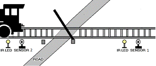
  • Practically, the two IR sensors are placed at left and right side of the railway gate. The distance between the two IR sensors is dependent on the length of the train. In general we have to consider the longest train in that route.
  • Now we’ll see how this circuit actually works in real time. In this image, we can see the real time representation of this project.
  • If the sensor 1 detects the arrival of the train, microcontroller starts the motor with the help of motor driver in order to close the gate.
  • The gate remains closed as the train passes the crossing.
  • When the train crosses the gate and reaches second sensor, it detects the train and the microcontroller will open the gate.

Advantages and Applications

  • An Automatic Railway Gate Control is implemented with very simple hardware and easy control.
  • Human intervention at level crossings can be removed with the help of this project and many railway level crossing accidents can be prevented.

Limitations

  • The system can be implemented more efficiently by incorporating more efficient sensor network.
  • A combination manual wireless control and sensors based control can be used for better operation.

Automatic Door Bell With Object Detection

We all have a doorbell at our homes. When a visitor comes to our house, he searches for the doorbell switch and then rings it to let us know his presence. If the who came to our house cannot find the doorbell or else if the person is so short that he cannot reach the doorbell, what can be done? How will it be if we use an automatic doorbell which rings as soon as a person arrives at our place? There are no more hassles. The person who comes to our house need not search for the doorbell and press it any more. If we install this automatic doorbell using object detection circuit, the circuit will automatically sense the presence of the person and it rings the doorbell.

Circuit Diagram of Automatic Door Bell Using Object Detection:


This circuit operates using a pair of ultrasonic transmitter and receiver modules which are used to detect the person and then if the person is detected, the door bell is automatically turned ON when the person is in-front of the door.
The ultrasonic transmitter operates at a frequency of about 40 Kilo-Hertz. That means it continuously transmits the ultrasonic waves of about 40KHz. The power supply should be moderate such that the range of the transmitter is only about one or two meters. If the transmitting power is less than one meter, then there is a chance that the person who is one meter away is not detected. Also, if the range is set to be very large, then it may lead to false triggering, meaning that, the objects far away from our door are considered as the visitors and the alarm rings. This can be a nuisance for us if the alarm rings for every object or person far away. So, to avoid both the problems, the transmitting power is kept to an optimum level.
The ultrasonic receiver module receives the power at the frequency same as that of the transmitter’s so that noise will be eliminated and we get less false triggering. The sensitivity of the receiver can be tuned by using the 500K-ohm variable resistor arranged as a pot in the circuit. By tuning this properly, we can achieve the desired results. The output of our circuit is given to a buzzer circuit which acts as a doorbell in our case. The receiver in this circuit uses IC LM324 which is internally has four op-amps. Out of the four op-amps, we are using only four of them and leaving the other one unused as it is not much required in our case. The three op-amps are used in cascaded arrangement to provide high gain as well as noise free output.
An opto coupler is used at the output to avoid any interaction between our circuit and the door bell.
Assemble the circuit on a PCB as compactly as possible and then attach it to your main door. Thats it! You may provide a power supply using a 9V DC adapter with filtered and regulated output. If the 9V adapter with regulated output is not available, then we recommend you to use a 12V unregulated DC adapter with 7809 voltage regulator.

Solar Tracking System

Generally, solar panels are stationary and do not follow the movement of the sun. Here is a solar tracker system that tracks the sun’s movement across the sky and tries to maintain the solar panel perpendicular to the sun’s rays, ensuring that the maximum amount of sunlight is incident on the panel throughout the day. The solar tracker starts following the sun right from dawn, throughout the day till evening, and starts all over again from the dawn next day. 


Fig. 1 shows the circuit of the solar tracking system. The solar tracker comprises comparator IC
LM339, H-bridge motor driver IC L293D (IC2) and a few discrete components. Light-dependent
resistors LDR1 through LDR4 are used as sensors to detect the panel’s position relative to the
sun. These provide the signal to motor driver IC2 to move the solar panel in the sun’s direction.
LDR1 and LDR2 are fixed at the edges of the solar panel along the X axis, and connected to
comparators A1 and A2, respectively. Presets VR1 and VR2 are set to get low comparator output
at pins 2 and 1 of comparators A1 and A2, respectively, so as to stop motor M1 when the sun’s
rays are perpendicular to the solar panel.
When LDR2 receives more light than LDR1, it offers lower resistance than LDR1, providing a
high input to comparators A1 and A2 at pins 4 and 7, respectively. As a result, output pin 1 of
comparator A2 goes high to rotate motor M1 in one direction (say, anti-clockwise) and turn the
solar panel.
When LDR1 receives more light than LDR2, it offers lower resistance than LDR2, giving a low
input to comparators A1 and A2 at pins 4 and 7, respectively. As the voltage at pin 5 of
comparator A1 is now higher than the voltage at its pin 4, its output pin 2 goes high. As a result,
motor M1 rotates in the opposite direction (say, clock-wise) and the solar panel turns.
Similarly,

Similarly, LDR3 and LDR4 track the sun along Y axis. Fig. 2 shows the proposed assembly for
the solar tracking system.
For more detail visit…
http://electronicsforu.com/electronicsforu/circuitarchives/view_article.asp?sno=745&article_type
=1&id=674&tt=unhot&b_type=new

Thursday, 13 August 2015

GSM Controlled Robot using Microcontroller

GSM controlled robot or SMS controlled robot is a wireless robot which performs the necessary actions by receiving a set of instructions in the form a Short Message Service (SMS). In this project we can control the robot directions like forward, backward, left and right by sending SMS from the mobile. Earlier, we have already seen the working of a DTMF Controlled Robot without using Microcontroller.
This project mainly consists of 2 sections, one is mobile unit and the other one is robot unit. The GSM modem which is fixed at the robot receives the messages sent by the mobile and gives the instructions to the microcontroller to control the robot directions. In this project, we interface 8051 microcontroller with GSM SIM 300. The protocol used for the communication between controller and GSM modem is UART (Universal Asynchronous Receiver-Transmitter). This system continuously checks for message to take the decision for controlling the robot.

GSM Controlled Robot Circuit Principle:

When we send the message from the mobile to the modem, GSM modem sends the below command serially to indicate that new message is received.
+CMTI: “SM”,3
In the above command number 3 indicates the location of the new message. Now we need to read this unread message to display it on LCD. The command to read the message from GSM modem is
at+cmgr=3
Here the number 3 indicates the location of the message to be read. After sending this command to GSM module, modem sends the below command serially.
+CMGR: “REC UNREAD”,”MD-WAYSMS”,,”13/05/20,15:31:48+34″
forward
In the above command “REC UNREAD” indicates that message is unread message, “MD-WAYSMS” indicates sender mobile number or name, 13/05/20 indicates the date, 15:31indicates time and forward is the content of the message.
From the above command, we need to extract message (forward) sent by the user. Now compare this message with predefined strings (forward, backward, left, right), based on result control the robot.

GSM Controlled Robot Block Diagram:

GSM Controlled Robot Block Diagram
GSM Controlled Robot – Block Diagram

GSM Controlled Robot using 8051 Microcontroller Circuit:

GSM Controlled Robot Circuit Diagram using 8051 Microcontroller
GSM Controlled Robot Circuit Diagram
Hardware Requirements:
  • 8051 Microcontroller
  • AT89C51 Programming board
  • Programming cable
  • 16*2 LCD
  • MAX 232 level converter
  • GSM sim 300 module
  • L293D motor driver
  • Robot
  • 9V DC batteries – 2
  • 5V power supply circuit
  • 0.1uF ceramic capacitors – 4
  • 33pF capacitors – 2
  • 10uF electrolytic capacitor
  • 12MHz crystal
  • 10k (1/4 watt) resistor
  •  Single pin connecting wires
Software Requirements:
  • Kiel U vision
  • Flash magic
  • Proteus

SMS Controlled Robot Circuit Design:

The major components used in the above circuit are microcontroller, motor driver, level converter, GSM module and robot. Here at89c51 microcontroller is used and it requires a power supply of positive 5V DC. In order to provide regulated 5V DC voltage to the controller, use 7805 power supply circuit. Here two 9V batteries are used, one is for giving the supply to the circuit and other is to run the DC motors.
In the above circuit, 16 x 2 LCD is connected to the PORT1 of the microcontroller in 4 bit mode. LCD data lines D4, D5, D6 and D7 are connected to P1.4, P1.5, P1.6 and P1.7 respectively and control pins are connected to P1.0, P1.1 and P1.2. Here it used to indicate the received message.
 GSM modem Tx and Rx pins are connected to the 13 and 14 pins of max232. Microcontroller TXD and RXD pins are connected to the 11 and 12 pins of level converter. Here max232 is a mediator between controller and GSM module and it is used to convert the voltage levels. To know more details about max232 refer Max232 Datasheet.
GSM module requires 5V power supply. In order to communicate with this GSM we need to send AT commands using serial communication (UART protocol). Use a baud rate of 9600 to communicate with GSM.
P2.0, P2.1, P2.2 and P2.3 pins of controller are connected to the l293d input pins and these pins are used to control the two DC motors. The operating voltage of this IC is 5V. Using this IC we can operate the 2 DC motors with a voltage ranging from 4.5 to 36V. We need to apply the motors supply at 8th pin of l293d. To know more about motor driver IC refer L293D Datasheet.

GSM Controlled Robot Circuit Working Algorithm:

  1. Initialize the LCD and UART protocol
  2. Continuously check for the command +CMTI: “SM”,3 (Location number) to know weather new message is received or not
  3. If you receive the command then store message location number.
  4. Now read that particular message and extract the body of the message
  5. Display the extracted content on LCD and compare this content with predefined strings.
  6. If matched then perform the necessary action on robot.
Use below code to read a new message from the GSM modem.
while (rx_data() ! = 0x0d);
while (rx_data() ! = 0x0a);
if (rx_data() == ‘+’)
{
if (rx_data() == ‘C’)
{
if (rx_data() == ‘M’)
{
if (rx_data() == ‘T’)
{
if (rx_data()==’I’)
{
while (rx_data() != ‘,’);
a = rx_data ();
delay_ms (10);
tx_string (“at”);
tx_data (0x0d);
tx_data (0x0a);
tx_string (“at + cmgf =1″);
tx_data (0x0d);
tx_data (0x0a);
tx_string (“at + cmgr =”);
tx_data (a);
tx_data (0x0d);
tx_data (0x0a);
while (rx_data() ! = 0x0a);
while (rx_data() != 0x0a);
while (rx_data() ! = 0x0a);
for (i=0; i<15; i++)
{
read [i]= rx_data();
}
lcd_stringxy(1,0,read);
delay_ms (5000);
}
}
}
}
}

How to Operate GSM Mobile Controlled Robot?

  1. Write the program to the GSM controlled robot project using keil software
  2. Now burn the program to the microcontroller with the help of flash magic.
  3. Give the connections as per the circuit diagram.
  4. Use power supply circuit to provide 5V DC to the microcontroller
  5. Insert the SIM (Subscriber Identity Module) to the GSM module.
  6.  Now switch on the supply
  7. Send SMS to the GSM module using other mobile
  8. Now you can see the same message on LCD.
  9.  If the received message match with any predefined string then robot moves accordingly.
Limitations of the Circuit:
  • Robot section must have the network to receive the commands wirelessly.
  • As there is no password any one can operate the robot by sending message.

Solar Battery Charger

Solar Battery Charger Circuit Principle:

Here the solar panel produces 12V DC. The charging current passes to LM317 voltage regulator through the diode D1. The output voltage and current are regulated by adjusting the adjust pin of LM317 voltage regulator.

Solar Battery Charger Circuit Diagram:

Solar Battery Charger Circuit Diagram

Circuit Components:
  • Solar panel – 12V
  • LM317 voltage regulator
  • DC battery
  • Diode – 1n4007
  • Capacitor – 0.1uF
  • Schottky diode – 3A, 50V
  • Resistors – 220, 680 ohms
  • Pot – 2K
  • Connecting wires

Solar Battery Charger Circuit Design:

The circuit uses a 12V solar panel and an adjustable voltage regulator LM317. Solar panel consists of 1.2V rated solar cells. Pot RV1 is used to set the output voltage to the battery. Diode D2 prevents the discharge of battery.
For 6V Application:
  • Output voltage: set for 7v
  • Input voltage:
    • Battery discharged (6v): 8.75V@1.5mA
    • Battery charged (7V): 9V min @10mA
For 12V Application:
  • Output voltage: set for 14v
  • Input voltage:
    • Battery discharged (12v): 14.75V min @ 1.5mA ( available from solar panel characterized for 12V operation).
    • Battery charged (14V): 16V min @ 10mA.
Power Dissipation:
In this project, power is limited because of the thermal resistance of LM317 voltage regulator and the heat sink. To keep the temperature below 125 degree Celsius, the power must be limited to 10W. LM317 voltage regulator internally has temperature limiting circuit so that if it gets too hot, it shuts down automatically.
When battery is charging, heat sink becomes warm. When completing the charging at maximum voltage, heat sink runs hot. This heat is because of excess power that not needed in the process of charging a battery.
Current Limiting:
As the solar panel provides constant current, it acts as a current limiter. Therefore the circuit does not need any current limiting.
Solar Charger Protection:
In this circuit, capacitor C1 protects from the static discharge. Diode D1 protects from the reverse polarity. And voltage regulator IC provides voltage and current regulation.
Solar Charger Specifications:
  • Solar panel rating: 20W (12V) or 10W (6V)
  • Vout range: 5 to 14V
  • Maximum power dissipation: 10W (includes power dissipation of schottky diode)
  • Typical drop out value: 2 to 2.75V (depends on load current)
  • Max current: 1.5A (internally it limited to 2.2A)
  • Voltage regulation: +/- 100mV

How to Operate this Solar Battery Charger Circuit?

  1. Give the connections according to the circuit diagram.
  2. Place the solar panel in sunlight.
  3. Now set the output voltage by adjusting pot RV1
  4. Check the battery voltage using digital multi meter.

Solar Battery Charger Circuit Advantages:

  • Adjustable output voltage
  • Circuit is simple and inexpensive.
  • Circuit uses commonly available components.
  • Zero battery discharge when no sunlight on the solar panel.

Solar Battery Charger Circuit Applications:

Limitations of this Circuit:

  1. In this project current is limited to 1.5A.
  2. The circuit requires high drop-out voltage.

Lead Acid Battery Charger

Introduction:
To charge a battery from AC we need a step down transformer, rectifier, filtering circuit, regulator to maintain the constant voltage then we can give that voltage to the battery to charge it. Think if you have only DC voltage and charge the lead acid battery, we can do it by giving that DC voltage to a DC-DC voltage regulator and some extra circuitry before giving to the lead acid battery. Car battery is also a lead acid battery.
SIMPLE LEAD ACID BATTERY CHARGER - Block Diagram
As seen in the DC voltage is given to the DC voltage regulator here we use LM317 which is a DC voltage regulator. The regulated DC out voltage is given to battery. There is also a trickle charge mode circuitry which will help to reduce the current when the battery is fully charged.

Components of Lead Acid Battery Charger Circuit:

LM317: LM317 is voltage regulator invented by Robert C. Dobkin and Robert J. Widlar in 1970.the main function of this voltage regulator is to regulate the voltage and give the constant voltage without any noise disturbance; for example if we have 42v and we want only 10v so to get this output we will give 42v to a voltage regulator and uninterrupted 10v. For LM317 there is no maximum voltage unless the difference between the input and output voltage should not exceed maximum differential voltage. The maximum differential voltage is around 40V and also it give exceed output current of 1.5A for 1.2v to 37V .it has three pins input, output and adjustable pin. In the adjustable we can adjust the difference between the input and output voltages. Minimum voltage should be 18V which is given as input voltage to the regulator.
Lead Battery: Lead Battery is a rechargeable battery in the 1857 by gaston plante. The main advantages of Lead battery is it will dissipate very little energy (if energy dissipation is less it can work for long time with high efficiency),it has very low energy to weight ratio, it can deliver high current’s and very low cost.

Lead Acid Battery Charger Circuit Diagram:

The circuit diagram can be seen below:
SIMPLE LEAD ACID BATTERY CHARGER - Circuit Diagram
Circuit Explanation:
  • The DC voltage is connected to the Vin of the LM317 in between we have connected the capacitors will be opened but if it had any AC noise it will remove it.
  • The Vout of the LM317 is given to the battery which is to be charged, pin1Adjustment pin of the LM317 is connected to the transistor Q1, Resistor R1, R2, R5 which will help to adjust the regulator.
  • The output of regulated voltage and current is controlled by the transistor Q1, resistor R1 and R2 and potentiometer R5.potentiometer which is used to set the charging current. Resistor R2 will have more current when the battery is getting charged. This will help to conduct the transistor Q1. The conduction of Q1 will help to adjust the voltage of LM317.
  • TRICKLE CHARGE MODE: in this mode if the battery is charged the reverse current will flow. If the LED has glown then we can say that battery is charged. The diode D2 will protect the LM317 from the reverse current. When the battery is fully charged it will reduce the charge current. If the charge current the transistor will get off so the voltage regulator cannot be adjusted.
NOTE:
  1. The battery should be charged with 1/10th it’s charging current.so the voltage regulator must generate 1/10th of the charging current produced by the battery
  2. Heat sink should be attached to the LM317 to the get the better efficiency.

Mobile Jammer Circuit


In the earlier post, we have studied about Simple FM Radio Jammer Circuit and its applications. Now, let us learn about one more interesting concept i.e. Cell Phone or Mobile Phone Jammer Circuit.

Simple Mobile Jammer Circuit Diagram:

Mobile Jammer Circuit Diagram
Simple Mobile Jammer Circuit Diagram

Cell Phone Jammer Circuit Explanation:

  • If you understand the above circuit, this circuit analysis is simple and easy. For any jammer circuit, remember that there are three main important circuits. When they are combined together, the output of that circuit will work as a jammer. The three circuits are
    1. RF amplifier.
    2. Voltage controlled oscillator.
    3. Tuning circuit.
  • So the transistor Q1, capacitors C4 & C5 and resistor R1 constitute the RF amplifier circuit. This will amplify the signal generated by the tuned circuit. The amplification signal is given to the antenna through C6 capacitor. Capacitor C6 will remove the DC and allow only the AC signal which is transmitted in the air.
  • When the transistor Q1 is turned ON, the tuned circuit at the collector will get turned ON. The tuned circuit consists of capacitor C1 and inductor L1. This tuned circuit will act as an oscillator with zero resistance.
  • This oscillator or tuned circuit will produce the very high frequency with minimum damping. The both inductor and capacitor of tuned circuit will oscillate at its resonating frequency.
  • The tuned circuit operation is very simple and easy to understand. When the circuit gets ON, the voltage is stored by the capacitor according to its capacity. The main function of capacitor is to store electric energy. Once the capacitor is completely charged, it will allow the charge to flow through inductor. We know that inductor is used to store magnetic energy. When the current is flowing across the inductor, it will store the magnetic energy by this voltage across the capacitor and will get decreased, at some point complete magnetic energy is stored by inductor and the charge or voltage across the capacitor will be zero. The magnetic charge through the inductor will decreased and the current will charge the capacitor in opposite or reverse polarity manner. Again after some period of time, capacitor will get completely charged and magnetic energy across the inductor will be completely zero. Again the capacitor will give charge to the inductor and becomes zero. After some time, inductor will give charge to capacitor and become zero and they will oscillate and generate the frequency.
  • This circle run upto the internal resistance is generated and oscillations will get stop. RF amplifier feed is given through the capacitor C5 to the collector terminal before C6 for gain or like a boost signal to the tuned circuit signal. The capacitors C2 and C3 are used for generating the noise for the frequency generated by the tuned circuit. Capacitors C2 and C3 will generate the electronic pulses in some random fashion (technically called noise).
  • The feedback back or boost given by the RF amplifier, frequency generated by the tuned circuit, the noise signal generated by the capacitors C2 and C3 will be combined, amplified and transmitted to the air.
  • Cell phone works at the frequency of 450 MHz frequency. To block this 450MHz frequency, we also need to generate 450Mhz frequency with some noise which will act as simple blocking signal, because cell phone receiver will not be able to understand to which signal it has been received. By this, we can able to block the cell phone signal from reaching the cell phones.
  • So here in the above circuit, we generated the 450 MHz frequency to block the actual cell phone signal. That’s what the above circuit will act as a jammer for blocking the actual signal.
Note:
  • This circuit will work in the range of 100 meters i.e. it can block the signals of cell phones with in 100 meters radius.
  • Usage of this type of circuits is banned in most of the countries. Usage of this circuit is illegal and if you caught by using this circuit, you can be imprisoned and also should pay large amount in the form of fine.
  • This circuit can be used in TV transmission and also for remote controlled toys or play things.
  • If the circuit is not working, just increase the resistor and capacitors values in the circuit. Increase the frequency of tuned circuit by using this formula F= 1/ (2*pi*sqrt (L*C)). Increase the inductor capacitor circuit components value for increasing the frequency.