GSM controlled robot or SMS controlled robot is a wireless robot which performs the necessary actions by receiving a set of instructions in the form a Short Message Service (SMS). In this project we can control the robot directions like forward, backward, left and right by sending SMS from the mobile. Earlier, we have already seen the working of a DTMF Controlled Robot without using Microcontroller.
This project mainly consists of 2 sections, one is mobile unit and the other one is robot unit. The GSM modem which is fixed at the robot receives the messages sent by the mobile and gives the instructions to the microcontroller to control the robot directions. In this project, we interface 8051 microcontroller with GSM SIM 300. The protocol used for the communication between controller and GSM modem is UART (Universal Asynchronous Receiver-Transmitter). This system continuously checks for message to take the decision for controlling the robot.
GSM Controlled Robot Circuit Principle:
When we send the message from the mobile to the modem, GSM modem sends the below command serially to indicate that new message is received.
+CMTI: “SM”,3
In the above command number 3 indicates the location of the new message. Now we need to read this unread message to display it on LCD. The command to read the message from GSM modem is
at+cmgr=3
Here the number 3 indicates the location of the message to be read. After sending this command to GSM module, modem sends the below command serially.
+CMGR: “REC UNREAD”,”MD-WAYSMS”,,”13/05/20,15:31:48+34″
forward
forward
In the above command “REC UNREAD” indicates that message is unread message, “MD-WAYSMS” indicates sender mobile number or name, 13/05/20 indicates the date, 15:31indicates time and forward is the content of the message.
From the above command, we need to extract message (forward) sent by the user. Now compare this message with predefined strings (forward, backward, left, right), based on result control the robot.
GSM Controlled Robot Block Diagram:
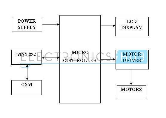
GSM Controlled Robot – Block Diagram
GSM Controlled Robot using 8051 Microcontroller Circuit:
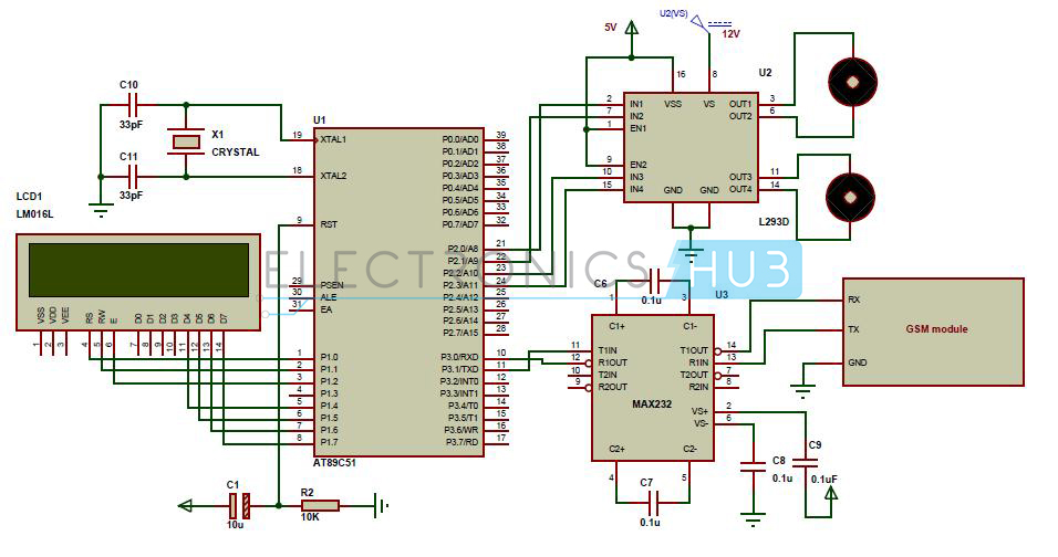
GSM Controlled Robot Circuit Diagram
Hardware Requirements:
- 8051 Microcontroller
- AT89C51 Programming board
- Programming cable
- 16*2 LCD
- MAX 232 level converter
- GSM sim 300 module
- L293D motor driver
- Robot
- 9V DC batteries – 2
- 5V power supply circuit
- 0.1uF ceramic capacitors – 4
- 33pF capacitors – 2
- 10uF electrolytic capacitor
- 12MHz crystal
- 10k (1/4 watt) resistor
- Single pin connecting wires
Software Requirements:
- Kiel U vision
- Flash magic
- Proteus
SMS Controlled Robot Circuit Design:
The major components used in the above circuit are microcontroller, motor driver, level converter, GSM module and robot. Here at89c51 microcontroller is used and it requires a power supply of positive 5V DC. In order to provide regulated 5V DC voltage to the controller, use 7805 power supply circuit. Here two 9V batteries are used, one is for giving the supply to the circuit and other is to run the DC motors.
In the above circuit, 16 x 2 LCD is connected to the PORT1 of the microcontroller in 4 bit mode. LCD data lines D4, D5, D6 and D7 are connected to P1.4, P1.5, P1.6 and P1.7 respectively and control pins are connected to P1.0, P1.1 and P1.2. Here it used to indicate the received message.
GSM modem Tx and Rx pins are connected to the 13 and 14 pins of max232. Microcontroller TXD and RXD pins are connected to the 11 and 12 pins of level converter. Here max232 is a mediator between controller and GSM module and it is used to convert the voltage levels. To know more details about max232 refer Max232 Datasheet.
GSM module requires 5V power supply. In order to communicate with this GSM we need to send AT commands using serial communication (UART protocol). Use a baud rate of 9600 to communicate with GSM.
P2.0, P2.1, P2.2 and P2.3 pins of controller are connected to the l293d input pins and these pins are used to control the two DC motors. The operating voltage of this IC is 5V. Using this IC we can operate the 2 DC motors with a voltage ranging from 4.5 to 36V. We need to apply the motors supply at 8th pin of l293d. To know more about motor driver IC refer L293D Datasheet.
GSM Controlled Robot Circuit Working Algorithm:
- Initialize the LCD and UART protocol
- Continuously check for the command +CMTI: “SM”,3 (Location number) to know weather new message is received or not
- If you receive the command then store message location number.
- Now read that particular message and extract the body of the message
- Display the extracted content on LCD and compare this content with predefined strings.
- If matched then perform the necessary action on robot.
Use below code to read a new message from the GSM modem.
while (rx_data() ! = 0x0d);
while (rx_data() ! = 0x0a);
if (rx_data() == ‘+’)
{
if (rx_data() == ‘C’)
{
if (rx_data() == ‘M’)
{
if (rx_data() == ‘T’)
{
if (rx_data()==’I’)
{
while (rx_data() != ‘,’);
a = rx_data ();
delay_ms (10);
tx_string (“at”);
tx_data (0x0d);
tx_data (0x0a);
tx_string (“at + cmgf =1″);
tx_data (0x0d);
tx_data (0x0a);
tx_string (“at + cmgr =”);
tx_data (a);
tx_data (0x0d);
tx_data (0x0a);
while (rx_data() ! = 0x0a);
while (rx_data() != 0x0a);
while (rx_data() ! = 0x0a);
for (i=0; i<15; i++)
{
read [i]= rx_data();
}
lcd_stringxy(1,0,read);
delay_ms (5000);
}
}
}
}
}
while (rx_data() ! = 0x0a);
if (rx_data() == ‘+’)
{
if (rx_data() == ‘C’)
{
if (rx_data() == ‘M’)
{
if (rx_data() == ‘T’)
{
if (rx_data()==’I’)
{
while (rx_data() != ‘,’);
a = rx_data ();
delay_ms (10);
tx_string (“at”);
tx_data (0x0d);
tx_data (0x0a);
tx_string (“at + cmgf =1″);
tx_data (0x0d);
tx_data (0x0a);
tx_string (“at + cmgr =”);
tx_data (a);
tx_data (0x0d);
tx_data (0x0a);
while (rx_data() ! = 0x0a);
while (rx_data() != 0x0a);
while (rx_data() ! = 0x0a);
for (i=0; i<15; i++)
{
read [i]= rx_data();
}
lcd_stringxy(1,0,read);
delay_ms (5000);
}
}
}
}
}
How to Operate GSM Mobile Controlled Robot?
- Write the program to the GSM controlled robot project using keil software
- Now burn the program to the microcontroller with the help of flash magic.
- Give the connections as per the circuit diagram.
- Use power supply circuit to provide 5V DC to the microcontroller
- Insert the SIM (Subscriber Identity Module) to the GSM module.
- Now switch on the supply
- Send SMS to the GSM module using other mobile
- Now you can see the same message on LCD.
- If the received message match with any predefined string then robot moves accordingly.
Limitations of the Circuit:
- Robot section must have the network to receive the commands wirelessly.
- As there is no password any one can operate the robot by sending message.